Overview
Now, thick-film audio power amplifier ICs are available
with pin-compatibility to permit a single PCB to be
designed and amplifier output capacity changed simply by
installing a hybrid IC. This new series was developed
with this kind of pin-compatibility to ensure integration
between systems everywhere. With this new series of IC,
even changes from 3-channel amplifier to 2-channel
amplifiers is possible using the same PCB. In addition,
this new series of ICs has a 6/3
drive in order to support
the low impedance of modern speakers.
Features
∑ Pin-compatible
STK400-000 series (3-channel, single package)
STK401-000 series (2-channel, single package)
∑ Output load impedance RL=6
/3
supported
∑ New pin arrangement
To simplify input/output pattern layout and minimize
the effects of pattern layout on operational
characteristics, pin assignments are grouped into blocks
consisting of input, output and power systems.
∑ Few external circuits
Compared to those series used until now, capacitors and
boot-strap resistors for external circuits can be greatly
reduced.
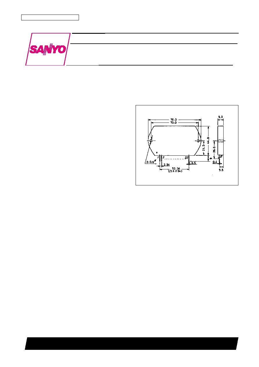
Package Dimensions
unit: mm
4086A
Thick Film Hybrid IC
D3096HA(OT)/12093YO No. 4340-1/9
[STK400-050]
SANYO Electric Co.,Ltd. Semiconductor Bussiness Headquarters
TOKYO OFFICE Tokyo Bldg., 1-10, 1 Chome, Ueno, Taito-ku, TOKYO, 110 JAPAN
AF Power Amplifier (Split Power Supply)
(30 W + 30 W + 30 W min, THD = 0.4%)
STK400-050
Ordering number : EN4340A
•
No. 4340-2/9
STK400-050
Specifications
Maximum Ratings
at Ta = 25∞C
Notes
∑ Use rated power supply for test unless otherwise specified.
∑ When measuring available time for load short-circuit and output noise voltage use transformer power supply indicated
below.
∑ Output noise voltage is represented by the peak value rms (VTVM) for mean reading. Use an AC stabilized power
supply (50 Hz) on the primary side to eliminate the effect of AC flicker noise.
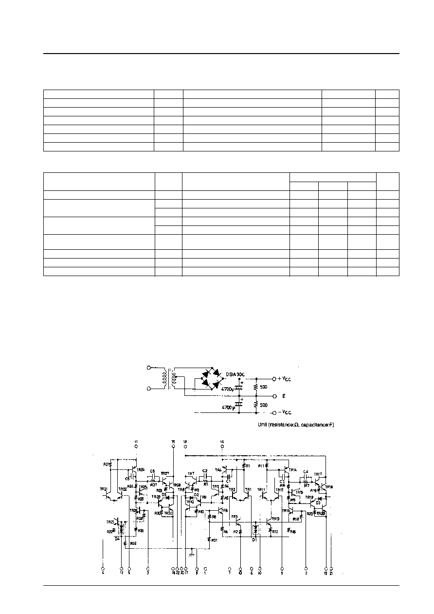
Internal Equivalent Circuit
Specified Transformer Power Supply
(RP-25 Equivalent)
Parameter
Symbol
Conditions
Ratings
Unit
Maximum supply voltage
V
CC
max
±39
V
Thermal resistance
j-c
Per power transistor
1.8
∞C/W
Junction temperature
Tj
150
∞C
Operating substrate temperature
Tc
125
∞C
Storage temperature range
Tstg
≠30 to +125
∞C
Available time for load short-circuit
t
s
V
CC
= ±26 V, R
L
= 6
, f = 50 Hz, P
O
= 30 W
1
s
Parameter
Symbol
Conditions
Ratings
Unit
min
typ
max
Quiescent current
I
CCO
V
CC
=± 31 V
30
90
150
mA
Output power
P
O
(1)
V
CC
= ±26 V, f = 20 Hz to 20 kHz, THD = 0.4%
30
35
W
P
O
(2)
V
CC
= ±22 V, f = 1 kHz, THD = 1.0%, R
L
= 3
30
35
W
Total harmonic distortion
THD (1)
V
CC
= ±26 V, f = 20 Hz to 20 kHz, P
O
= 1.0 W
0.4
%
THD (2)
V
CC
= ±26 V, f = 1 kHz, P
O
= 5.0 W
0.01
%
Frequency response
f
L
, f
H
V
CC
= ±26 V, P
O
= 1.0 W,
dB
20 to 50 k
Hz
Input impedance
r
i
V
CC
= ±26 V, f = 1 kHz, P
O
= 1.0 W
55
k
Output noise voltage
V
NO
V
CC
= ±31 V, Rg = 10 k
1.2
mVrms
Neutral voltage
V
N
V
CC
= ±31 V
≠70
0
+70
mV
+0
≠3
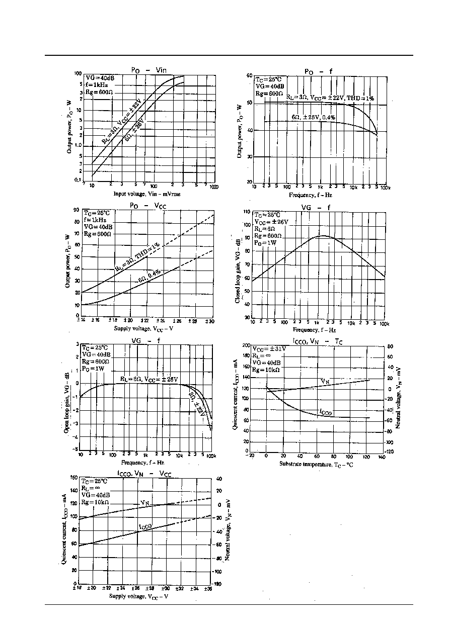
Operating Characteristics
at Ta = 25∞C, R
L
= 6
, Rg = 600
, VG = 40dB, R
L
(non-inductive)
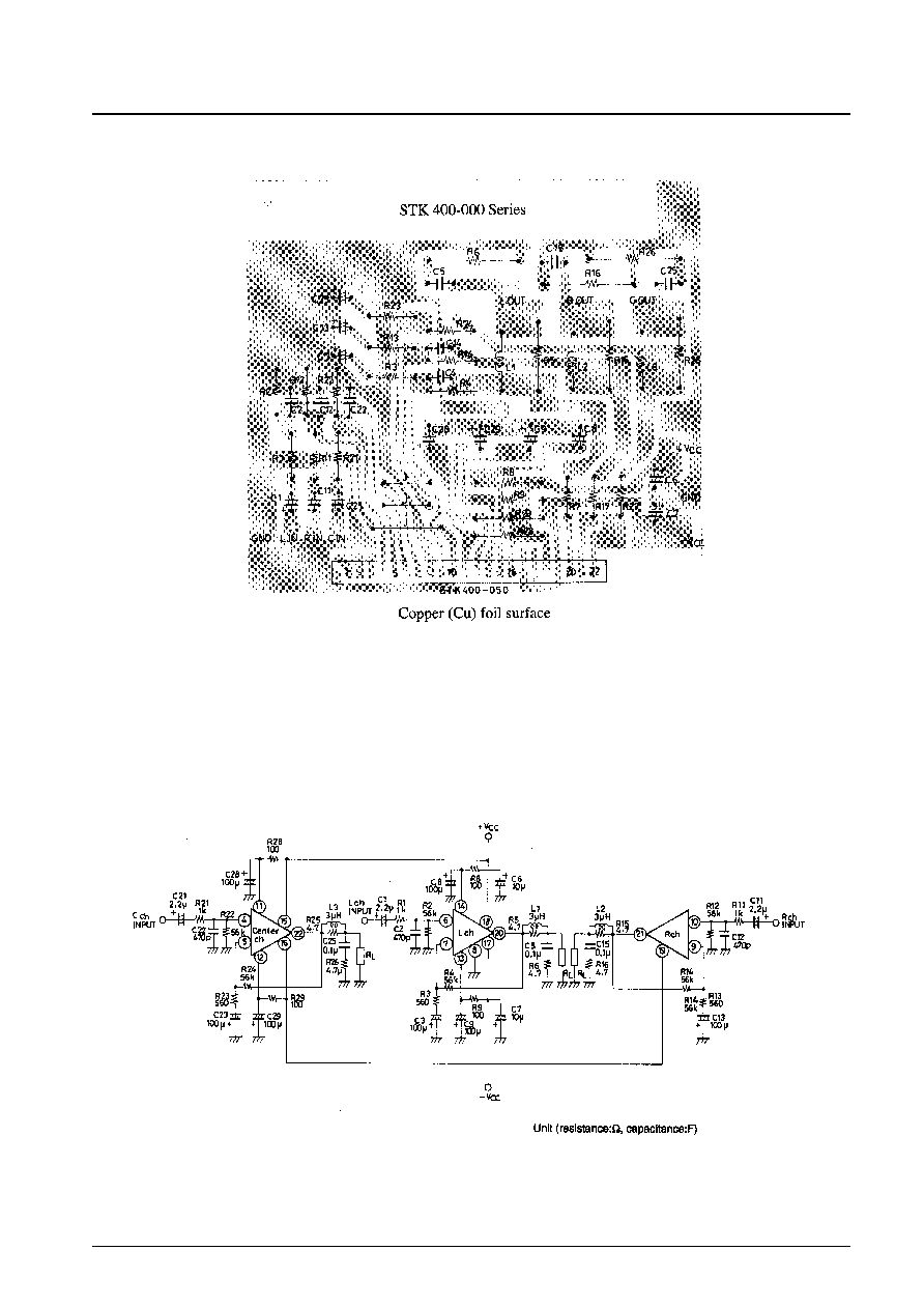
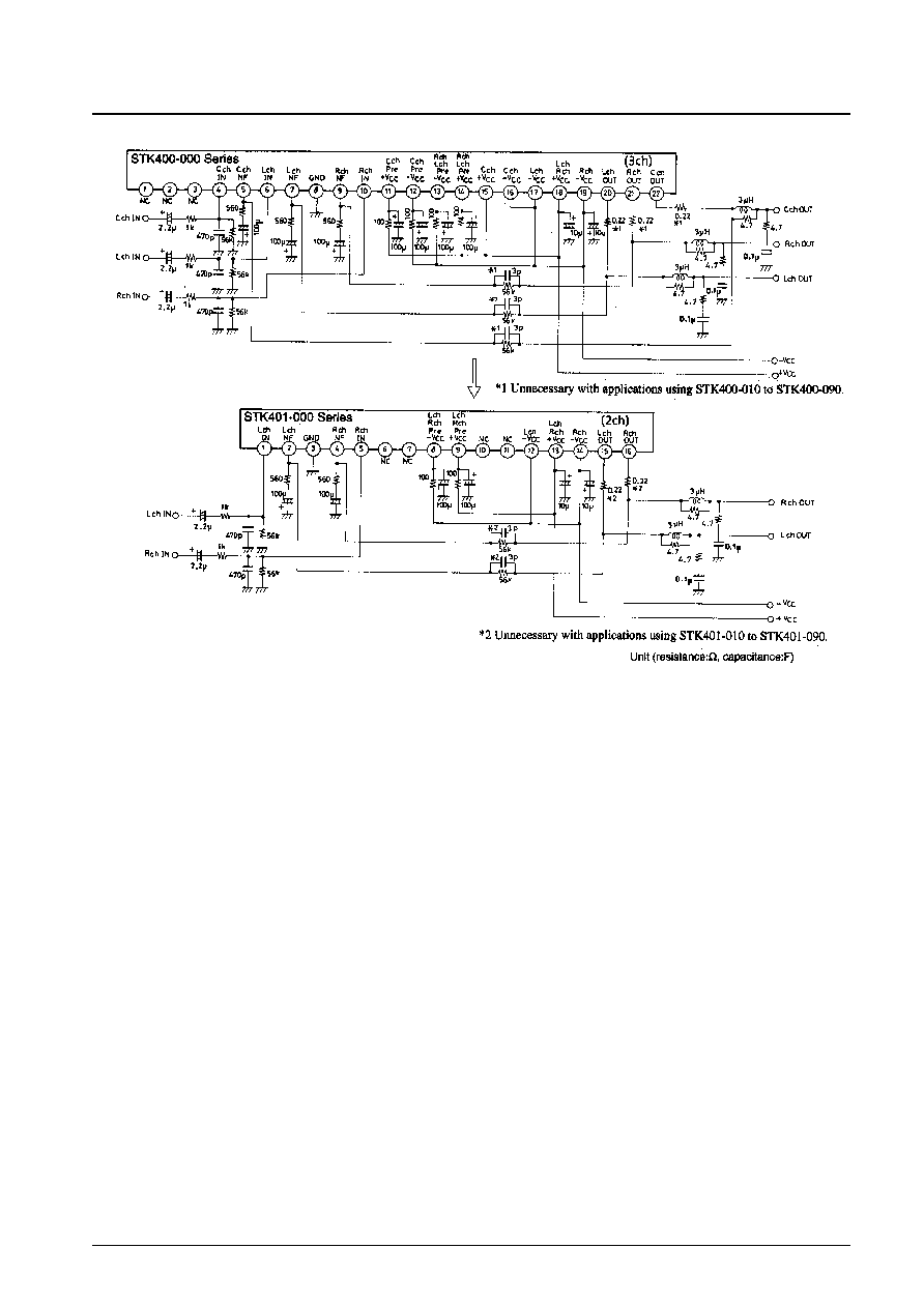
Pattern Example for PCB used with either 2- or 3-channel Amplifiers.
Sample Application Circuit
In the STK401-000 series, pin No. 6 corresponds to pin No. 1.
No. 4340-3/9
STK400-050
No. 4340-4/9
STK400-050
Description of External Circuits
C1, 11, 21
For input coupling capacitor. Used for current blocking. When capacitor reactance with low
frequency is increased, the reactance value should be reduced in order to reduce the output
noise from the signal resistance dependent 1/f noise. In response to the popping noise which
occurs when the system power is turned on, C1 and C11 which determine the decay time
constant on the input side are increased while C3, C13 and C23 on the NF side are decreased.
C2, 12, 22
For input filter capacitor. Permits high-region noise reduction by utilizing filter constructed with
R1, R11 and R21.
C3, 13, 23
For NF capacitor. This capacitor determines the decline of the cut-off frequency and is
calculated according to the following equation.
f
L
=
1
2
X C3 (13, 23,) X R3 (13, 23)
For the purpose of achieving voltage gains prior to reduction, it is best that C3, C13 and C23 are
large. However, because the shock noise which occurs when the system power is turned on
tends to increase, values larger than those absolutely necessary should be avoided.
C5, 15, 25
For oscillation prevention capacitor. A Mylar capacitor with temperature and frequency features
is recommended.
C6, 7
For oscillation prevention capacitor. To ensure safe IC functioning, the capacitor should be
installed as close as possible to the IC power pin to reduce power impedance. An electrolytic
capacitor is good.
C8, 9, 28, 29
For decoupling capacitor. Reduces shock noise during power up using decay time constant
circuits with R8, R9, R28 and R29 and eliminates components such as ripples crossing over into
the input side from the power line.
R1, 11, 21
For input filter applied resistor.
R2, 12, 22
For input bias resistor. The input pin is biased to zero potential. Input impedance is mostly
decided with this resistance value.
R3, 13, 23
R4, 14, 24
For resistors to determine voltage gain (VG). We recommend a VG = 40 dB using R3, R13, R23
= 560
and R4, R14 and R24 = 56
. VG adjustments are best performed using R3, R13 and
R23. When using R4, R14 and R24 for such purposes, R4, R14 and R24 should be set to equal
R2, R12 and R22 in order to establish a stable VN balance.
R5, 15, 25
For oscillation prevention resistor.
R6, 16, 26
For oscillation prevention resistor. This resistor's electrical output resides in the signal frequency
and is calculated according to the following formula.
P R6 (16, 26) =
(
V
CC
max/
2
)
2
X R6 (16, 26)
1/2
fC5 (15, 25) + R6 (16, 26)
f = output signal frequency upper limit
R8, 9, 28, 29
For ripple filter applied resistor. PO max, ripple rejection and power-up shock noise are modified
according to this value. Set the electrical output of these resistors while keeping in mind the flow
of peak current during recharging to C8, C9, C28 and C29 which function as pre-drive TR control
resistors during load shorts.
L1, 2, 3
For oscillation prevention coil. Compensates
phase dislocation caused by load capacitors
and ensures stable oscillation.
No. 4340-5/9
STK400-050
Series Configuration
V
CC
max1
V
CC
max2
V
CC
1
V
CC
2
STK400-010
10W X 3
STK401-010
10W X 2
--
±27
±18
±14
STK400-020
15W X 3
STK401-020
15W X 2
--
±29
±20
±16
STK400-030
20W X 3
STK401-030
20W X 2
--
±34
±23
±19
STK400-040
25W X 3
STK401-040
25W X 2
--
±36
±25
±21
STK400-050
30W X 3
STK401-050
30W X 2
--
±39
±26
±22
STK400-060
35W X 3
STK401-060
35W X 2
--
±41
±28
±23
STK400-070
40W X 3
STK401-070
40W X 2
0.4
--
±44
±30
±24
STK400-080
45W X 3
STK401-080
45W X 2
--
±45
±31
±25
STK400-090
50W X 3
STK401-090
50W X 2
--
±47
±32
±26
STK400-100
60W X 3
STK401-100
60W X 2
--
±51
±35
±27
STK400-110
70W X 3
STK401-110
70W X 2
±56.0
--
±38
--
--
--
STK401-120
80W X 2
±61.0
--
±42
--
--
--
STK401-130
100W X 2
±65.0
--
±45
--
--
--
STK401-140
120W X 2
±74.0
--
±51
--
V
CC
max1
R
L
= 6
V
CC
max2
R
L
= 6
to 3
operation
V
CC
1
R
L
= 6
operation
V
CC
2
R
L
= 3
operation
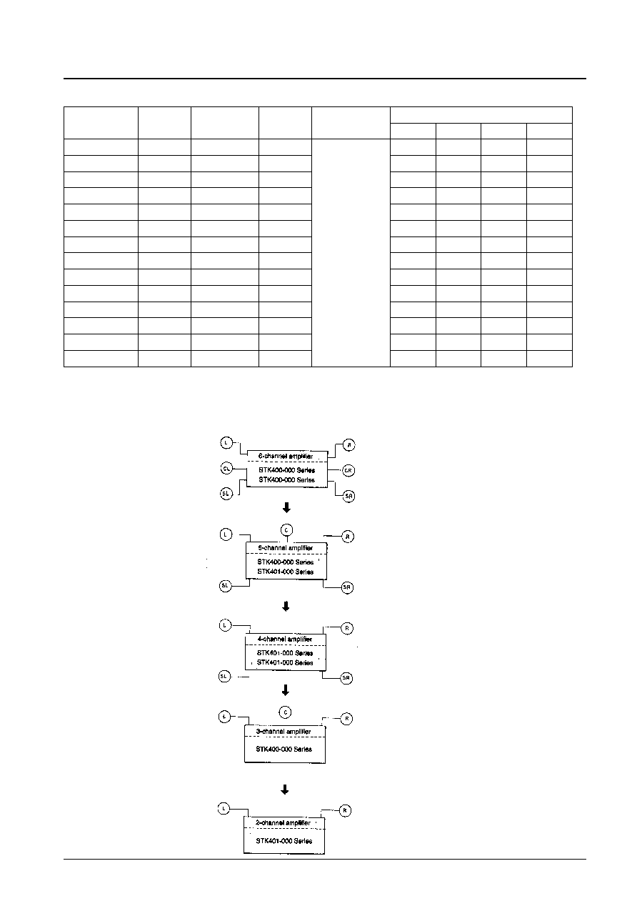
Example of Set Design for Common PCB
Supply voltage
3ch Amp
IC Name
Fixed
Standard
Output
2ch Amp
IC Name
Fixed
Standard
Output
THD [%]
f = 20 to 20kHz
No. 4340-6/9
STK400-050
External Circuit Diagram
Heat Radiation Design Considerations
The radiator thermal resistance
c-a required for total substrate power dissipation Pd in the STK400-050 is determined as:
Condition 1: IC substrate temperature Tc not to exceed 125∞C.
Pd
x
c-a+Ta <125∞C ∑∑∑∑∑∑∑∑∑∑∑∑∑∑∑∑∑∑∑∑∑∑∑∑∑∑∑∑∑∑∑ (1)
where Ta is set assured ambient temperature.
Condition 2: Power transistor junction temperature Tj not to exceed 150∞C.
Pd
x
c-a+Pd/N
x
j-c+Ta<150∞C∑∑∑∑∑∑∑∑∑∑∑∑∑(2)
where N is the number of power transistors and
j-c the thermal resistance per power transistor chip.
However, power transistor power consumption is Pd equally divided by N units.
Expressions (1) and (2) can be rewritten based on
c-a to yield:
c-a<(125≠Ta)/Pd ∑∑∑∑∑∑∑∑∑∑∑∑∑∑∑∑∑∑∑∑∑∑∑∑∑∑∑∑∑∑∑∑∑∑∑∑∑∑(1)'
c-a<(150≠Ta)/Pd≠
j-c/N∑∑∑∑∑∑∑∑∑∑∑∑∑∑∑∑∑∑∑∑∑∑∑∑∑∑(2)'
The required radiator thermal resistance will satisfy both of these expressions.
From expressions (1)' and (2)', the required radiator thermal resistance can be determined once the following
specifications are known:
∑
Supply voltage
V
CC
∑
Load resistance
R
L
∑
Assured ambient temperature
Ta
The total substrate power consumption when STK400-050 V
CC
is ±26 V and R
L
is 6
, for a continuous sine wave
signal, is a maximum of 70W (Fig. 1). In general, when this sort of continuous signal is used for estimation of power
consumption, the Pd used is 1/10th of P
O
max (slight variation depending on safety standard).
Pd=42.5W (1/10 P
O
max=during 3W)
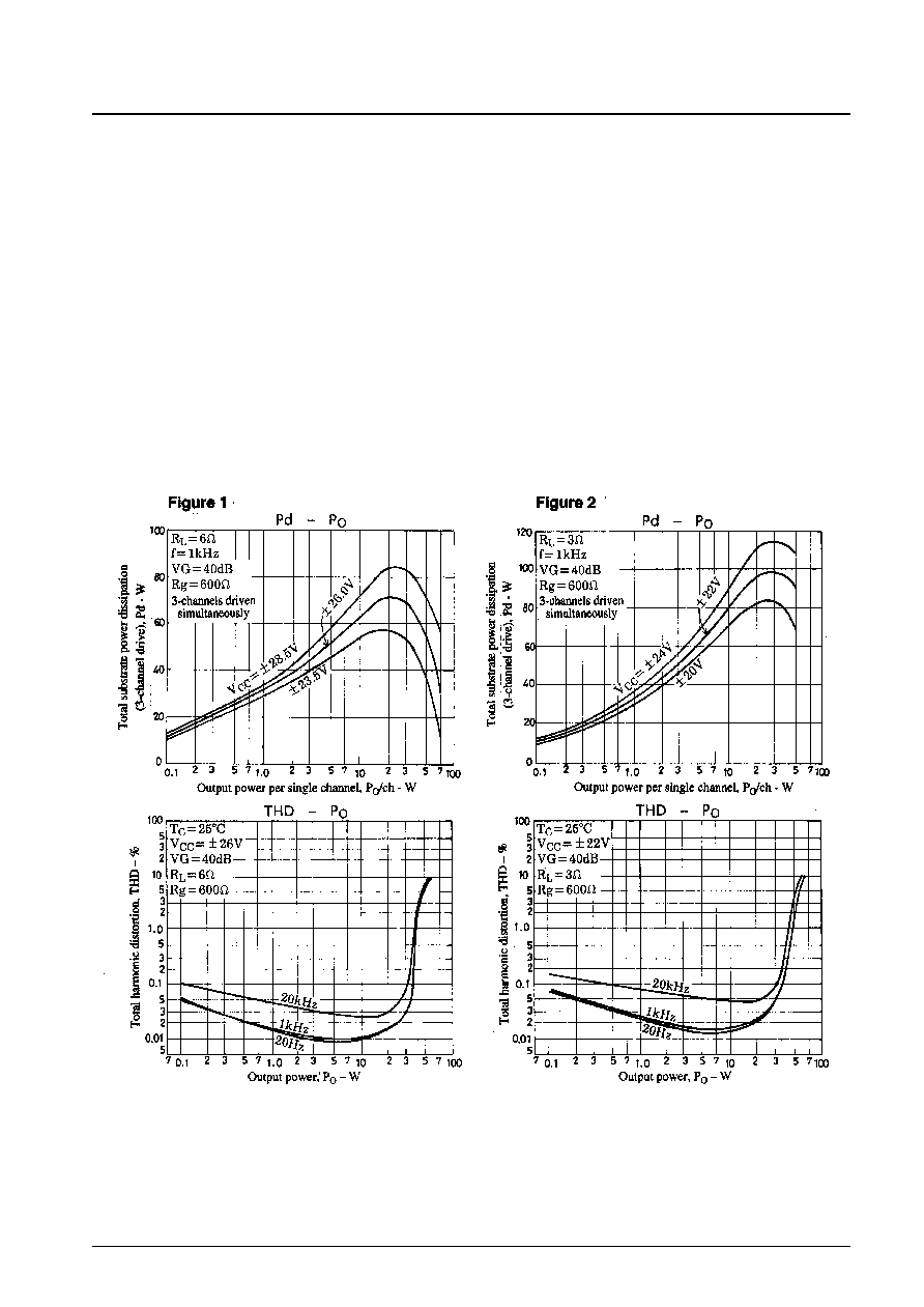
The STK400-050 has six power transistors, so the thermal resistance per transistor
j-c is 1.8∞C / W. With an assured
ambient temperature Ta of 50∞C, the required radiator thermal resistance
c-a would be:
From expression (1)'
c-a <(125≠50)/42.5
<1.76
From expression (2)'
c-a <(150≠50)/42.5≠1.8/6
<2.05
To satisfy both, 1.76∞C/W is the required radiator thermal resistance.
Figure 2 illustrates Pd - P
O
when the V
CC
of STK400-050 is ±19V and R
L
is functioning at 3
.
Pd = 51W (1/10 P
O
max = during 3W)
From expression (1)'
c-a <(125≠50)-51
<1.47
From expression (2)'
c-a <(150-50)/51-1.8/6
<1.66
To satisfy both, 1.47∞C / W is the required radiator thermal resistance. This design example is based on a fixed voltage
supply, and will require verification within your specific set environment.
No. 4340-7/9
STK400-050
No. 4340-8/9
STK400-050

No. 4340-9/9
STK400-050
This catalog provides information as of July, 1997. Specifications and information herein are subject to change
without notice.
s
No products described or contained herein are intended for use in surgical implants, life-support systems, aerospace
equipment, nuclear power control systems, vehicles, disaster/crime-prevention equipment and the like, the failure of
which may directly or indirectly cause injury, death or property loss.
s
Anyone purchasing any products described or contained herein for an above-mentioned use shall:
Accept full responsibility and indemnify and defend SANYO ELECTRIC CO., LTD., its affiliates, subsidiaries and
distributors and all their officers and employees, jointly and severally, against any and all claims and litigation and all
damages, cost and expenses associated with such use:
Not impose any responsibility for any fault or negligence which may be cited in any such claim or litigation on
SANYO ELECTRIC CO., LTD., its affiliates, subsidiaries and distributors or any of their officers and employees
jointly or severally.
s
Information (including circuit diagrams and circuit parameters) herein is for example only; it is not guaranteed for
volume production. SANYO believes information herein is accurate and reliable, but no guarantees are made or implied
regarding its use or any infringements of intellectual property rights or other rights of third parties.